The Modular Synthesizer Project
What is a modular synthesizer?
Most music producers work in a digital audio workstation (DAW), such as Ableton, Logic Pro, GarageBand, and FL Studio. I have spent many hours working with these tools; and, while making music is fun, searching through menus and windows is not the approach I want to take for music production anymore. Fortunately, a recent “DAW-less” movement has inspired me to reach for a solution: modular synthesizers. Their goal is to remove the personalized computer from the workflow, replacing a screen, mouse, and keyboard for knobs, switches, faders, and audio cables.
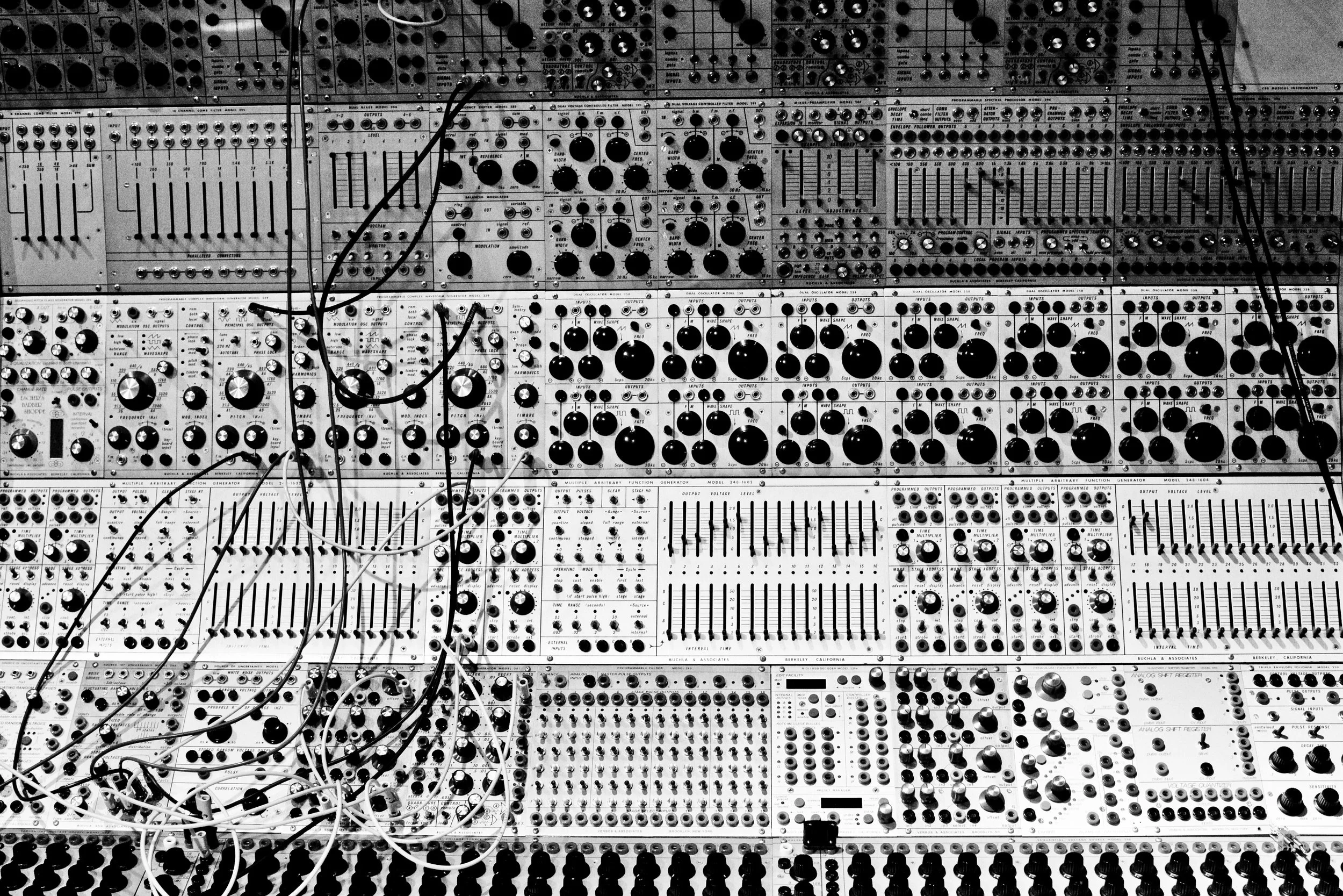
A modular synthesizer is a different kind of computer: one for sound design, electronic music-making, and experimentation. This synthesizer consists of multiple programmable “modules”, each serving a specific signal processing role. A simple modular synthesizer can be composed of an oscillator, envelope generator, and sequencer. However, this is typically not powerful enough to create evocative music or sounds. The beauty of a modular synthesizer is that it is modular, meaning it can be expanded to be as complex as the user intends. After all, each module is a circuit for processing a voltage signal, which will eventually drive a speaker to produce sound.
A wall of modules composing a modular synthesizer. Modules are programmed using patch cables. Source
The signal processing possibilities are endless. Well, at least until your wallet is empty. Modules can be expensive, especially for a college student. However, I’m not going to let that stop me from building an expansive modular synthesizer.
PCB Fabrication
Why PCB?
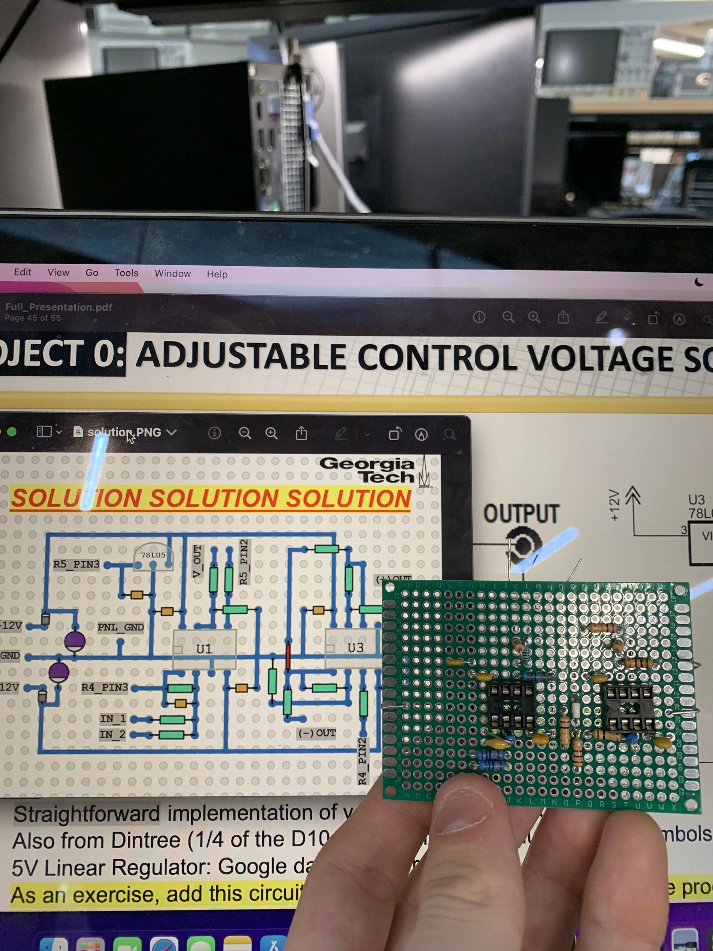
Originally, my first method to circuit building was protoboarding. For simple, one-off designs, creating a PCB design and waiting for its fabrication can be more time consuming than building a protoboard version. However, since realizing multiple copies of the same module is useful for a large system, I’ve moved from protoboarding to PCB design. I am also fortunate enough to have the tools to fabricate my own PCBs on campus, so I don’t need to pay for a fab house service + shipping.
Fabricating On Campus
The Hive Interdisciplinary Design Commons (IDC) at Georgia Tech is a makerspace equipped with hardware to build practically any project: 3D printers, soldering stations, laser cutters, milling machines, and (my favorite) LPKF tools for PCB fabrication. Over the summer of 2022, I became best friends with the ProtoLaser U4 and ProtoMat, despite much resistance.
The PCB fabrication machines are the only ones that require training and testing before using. This consists of passing an online test and fabricating a given design in-person within 2 hours. The interface for these machines are also clunky and buggy - it's easy for things to go wrong.
Because of this, many people prefer to send their designs to fab houses, such as JLCPCB. In fact, I was told multiple times that my time would be better spent doing this instead. Deep down, I know that this is true. The amount of hours I've dedicated to learning the machines could have been spent earning money for professional fabrication overseas; yet, I regret nothing.
The experience of creating a PCB from a large FR4 substrate within an hour gives a sense of ownership and accomplishment. Overseeing my PCBs has also improved my designs by exposing practical flaws. In this way, fabrication and design has been a positive feedback loop: fabricating a board, analyzing issues, returning to the design for fixes, repeat. I am very fortunate to have access to LPKF tools (for free!) and I thank the people at the Hive for this amazing opportunity.
The General Process
I won't describe all the steps required in software for each machine. This page is intended for quickly documenting the process, rather than educating with details.
Fabrication begins with setting up the ProtoMat with my design files for drilling holes in the substrate. Technically, the ProtoMat can also mill traces, but kills drills fast and has inferior accuracy to the ProtoLaser.
Once drilling is complete, the substrate is removed and its fiducial holes are smoothed. This is preparation for the ProtoLaser, which uses a small camera to aline itself with human placement. The ProtoLaser then hatches and heats the design on the substrate for each side.
After this job is complete, the circuit returns to the ProtoMat to be cut out of the substrate.
Chaos in the PCB
Fabrication on campus is far from flawless. I’ve had multiple boards ruined from bad ProtoLaser jobs. This typically involves incomplete traces, where the machine’s heating job was not enough for certain copper segments to curl off the substrate. Because of this, I inspect my boards through every step of the process under a microscope. It is very difficult to achieve the perfect PCB - I have tried. Even after reading through manuals and debugging the machine with multiple boards, the frequency of issues can only be mitigated. As of late, I have been tinkering with my PCB designs to be both machine and human friendly.
Board jobs used to find optimal tool settings in the ProtoLaser.
PCB Design
First Attempts
I use Autodesk's Eagle software for PCB design. On my first three attempts (two failures), I didn’t realize that I live in an advantageous 3D space. Instead, I foolishly puzzled together a single-sided layout for a 2-channel mixer.
Discovering The Third Dimension
I was not happy with my first design of the mixer, so I tried again with a double-sided board. I decided that one side will be my power rails with a ground pour, while the other for signal traces. I also made a design for adding additional channels to the mixer (this system is modular after all).
Fixing Practical Issues
When I began soldering components, I realized that, though I liked how my new PCBs looked, soldering was difficult. The small isolation between pads and the plane made it easy to create accident short-circuits. The small pads and traces made it easy to apply too much heat and curl copper off the substrate. There were also components, such as the capacitors in the right image below, that did not fit as I intended. I am still fixing these practical flaws in my designs whenever I realize them through soldering. This is also part of the recursive process I mentioned earlier.
Enjoying Professional Fabrication
Taking a break from my in-house PCBs, I’ve made some regular PCB designs for a LFO (low-frequency oscillator), Ring Modulator, and Wavefolder.
Test & Debug
After soldering all the components to a PCB, the next step is to hook up any potentiometers, faders, switches, and LEDs via breadboard, connect the function generator to some inputs, and scope the outputs.
Testing LFO
Testing Ringmod
Testing Wavefolder w/ FFT shown
Testing Wavefolder’s control voltage inputs
Testing four-pole VCF
Fruits of Labor
The last thing to do is create a panel and hook everything up to it for the final product. One of the most recent additions to the Hive’s inventory is the FabLight: a metal lazer cutter. Notable thanks to Selena Lin for working with me to create metal panels on the FabLight for these modules!
I’d also like to thank Professor Aaron Lanterman for mentoring me, as well as featuring the LFO and Wavefolder on his Lantertronics YouTube channel.
Closing Statements
There is still a lot of progress that needs to be made to fulfill my dream, but it has been so fulfilling to go from a schematic, to PCB design, to populated PCB, to a fully-functioning and beautiful module. As of now, I am leading the Synthesizer Education Project at Georgia Tech, working with other students to build a modular synthesizer which will be used as demonstration in ECE and music classes. I will continue to work on this project and post progress periodically. Thanks!


